Complete Semiconductor for Test Services
from ASIC Design to the Market
Microtest Group offers complete supply chain management, ensuring full traceability, reliable timelines, and minimized risks while optimizing logistics across external suppliers.

- Microtest Group supports customers with end-to-end services:
- Outsourced Design Service
- IP Blocks Design/Portfolio
- Full ASIC (Application-Specific Integrated Circuit) / ASSP (Application specific standard product) Design.
During the ASIC design stage, Microtest can support on the Design for Testability (DFT), reducing complexity and costs in later testing phases.

In this stage, Microtest acts as the main and sole point of contact through its reliable network, managing the complex process of engagement and integration with the Silicon Foundry, and ensuring efficient communication and oversight.

Microtest offers a true end-to-end approach to test solution development, acting as the single point of contact from initial design to hardware production. Thanks to the Group’s integrated supply chain, Microtest simplify the process for our clients by managing every phase internally — from concept to manufacturing.
We design and develop customized test solutions for the DUT through key internal activities:
- Development of the test program, including continuity testing, power consumption, scan test, and functional tests
- Debugging, validation, and release of the final test program, ready for operational use
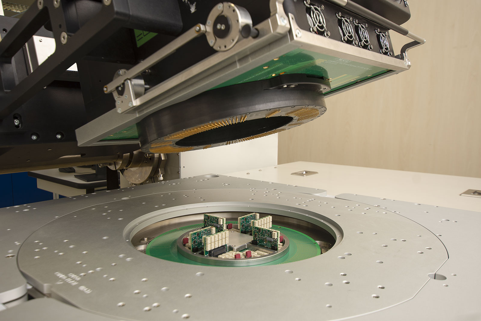
- Seamless transition to testing hardware (load boards or socket boards and probe cards), fully manufactured within our Group
This integrated workflow ensures faster delivery, higher reliability, and reduced complexity for our customers.

During the characterization tests on wafer and on packaged devices, electrical functional measurements and analyses are performed. These tests determine whether the device has been correctly designed, if process parameters affect its operation, and how the device’s performance changes under varying environmental, electrical and stress conditions.
Among the characterization tests performed by Microtest:
- CORNER LOT (Process, Voltage and Temperature, PVT)
- Voltage Temperature on wafer and packaged devices
- Radiation Test (for rad-hard applications).
RADIATION TEST
Thanks to a very small and portable ATE configuration (Hatina + DMT), Microtest allows to reuse the characterization test program during the radiation test. We can boast more than 10 years of experience on radiation test with special patented solution to heat and cold test in vacuum chambers.
- Access to highly qualified laboratories for radiation activity for SEE and TID on mixed-signal devices
- Running cooperation with companies qualified in physics sciences for beam management
- Standardized and consolidated radiation test flow
- Real-Time Software for SEL, SET, SEU analysis directly on the facility during the irradiation

Microtest acts as a single point of contact throughout the packaging and assembly phase, involving external partners, ensuring full alignment with test requirements and production standards.
Thanks to our consolidated network and internal coordination capabilities, we simplify interactions and reduce complexity for our clients, managing every step from design to final assembly with full traceability and accountability.

Qualification and reliability testing are essential to demonstrate device compatibility with specific application areas, particularly for safety-critical environments (industrial, automotive, medical, defense & aerospace).
The main types of qualifications are:
- Lifetime/reliability (Burn-In, HTOL – High Temperature Operating Life, LTOL, ESD, Solderability Test
- Environmental Stress Test (Temp Cycling and Temp. Shock, HAST — Highly Accelerated Stress Test, THB – Temperature Humidity Bias, HTRB – High Temperature Reverse Bias, High Voltage, Humidity, Temp Reverse Bias – HV-H3TRB)
- Mechanical Stress Test (Vibration, Shock, Constant Acceleration)

As volumes increase, Microtest focuses on optimizing key parameters:
- Parallelism (simultaneous device testing)
- Test Time per individual touch-down (Test Time Reduction)
- Production Yield (Yield Improvement)
- Burn-In


Microtest may support with many capabilities, including:
- Verification of History
- Anamnesis
- Curve Tracing, Electrical Characterization
- Fault Characterization
- X-Ray Microscopy (2D & 3D)
- Scanning Acoustic Microscopy (SAM)
- Decapsulation
- Failure Localization (EMMI, OBIRCH)
- Optical Microscopy
- Scanning Electron Microscopy (SEM)
- Energy Dispersive X-Ray Analysis (EDX)
- Metallographic Cross Sectioning
- Focused Ion Beam (FIB) Cross Section
- Infrared Spectroscopy (FTIR)
- Suggestions for Improvement
Why Microtest
Global Operations and Supply Chain
Our global test floors enhance risk mitigation and supply chain efficiency, ensuring closer proximity to customers for optimized operations. This is particularly crucial for semiconductor testing and component qualification.

Equipment and Advanced Testing Capabilities
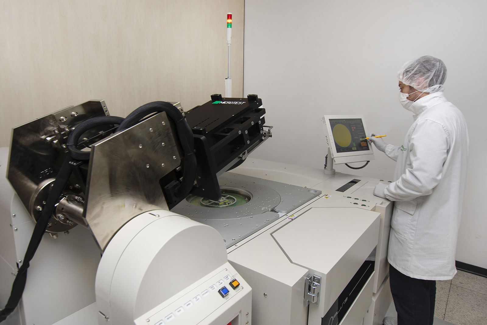
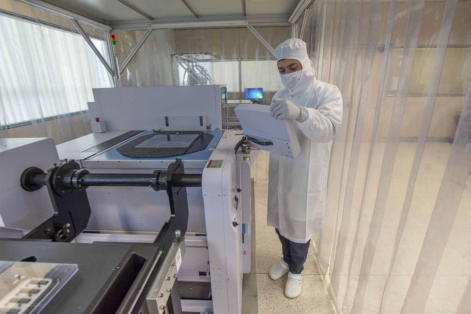
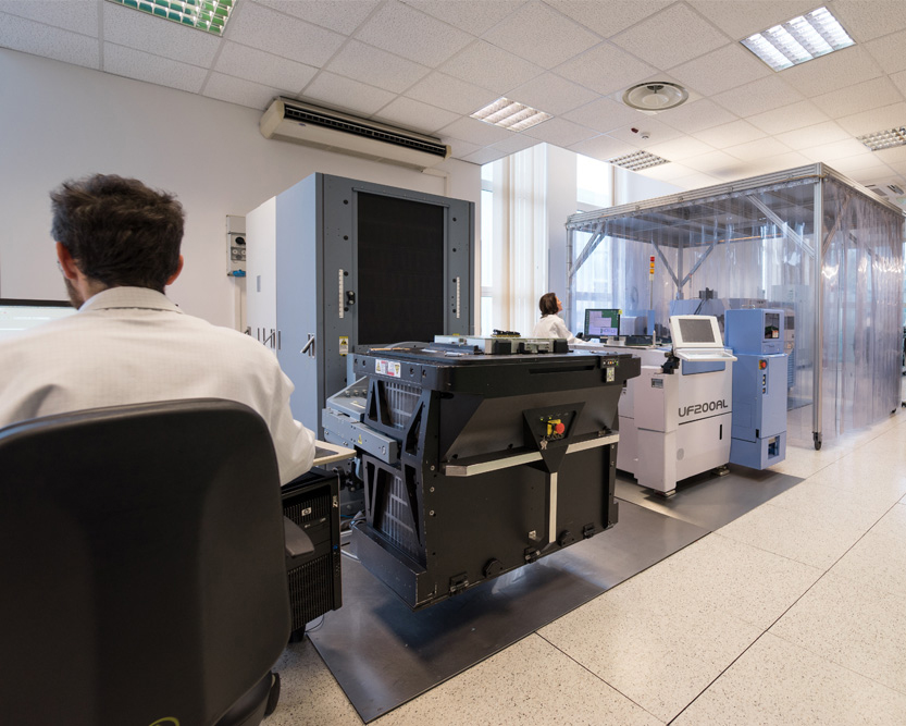
The test floors are fully equipped in clean room environments. We possess comprehensive expertise in a full range of ATE equipment (Automatic Test Equipment), offering advanced testing capabilities and reliable testing, which are fundamental for IC verification.

Multidisciplinary engineering team
Our multidisciplinary engineering team covers electronics, testing, mechanics, automation, and software development. Our test engineers are promptly available to support every phase of semiconductor production and process optimization.

Flexible Production and Management Solutions
We offer flexible production solutions for companies of all sizes, from start-ups to large players requiring mass production. Microtest Group provides complete supply Chain management, ensuring full traceability, reliable timelines, and minimized production risks, while optimizing component logistics.

Years of Experience and Compliance
With over 25 years of excellence in the Automotive testing, Medical, Aerospace, Industrial testing, Security, Scientific, and Consumer sectors. We are fully compliant with industry standards, providing high test quality across all regulated markets.

Continuous 24/7 Operation
24/7 operations across all test centers, with continuous shifts running 365 days a year, guarantee uninterrupted service. We maximize test efficiency and reliability, which are vital for semiconductor test services and automotive testing.


Equipment available
Microtest Group has a range of vendor-agnostic equipment designed to cover a broad spectrum of devices and applications across multiple markets, while ensuring operational flexibility and scalability in production volumes.
Some of the available equipment includes:
- Microtest Hatina GP
- Microtest DMT EVO (different configurations including µWave option)
- Teradyne J750
- Teradyne uFlex
- Teradyne UltraFlex
- Teradyne Integra Flex
- High volume Microtest Celsius 3T handler
- Exclusive Microtest Ovenless Burn-In system
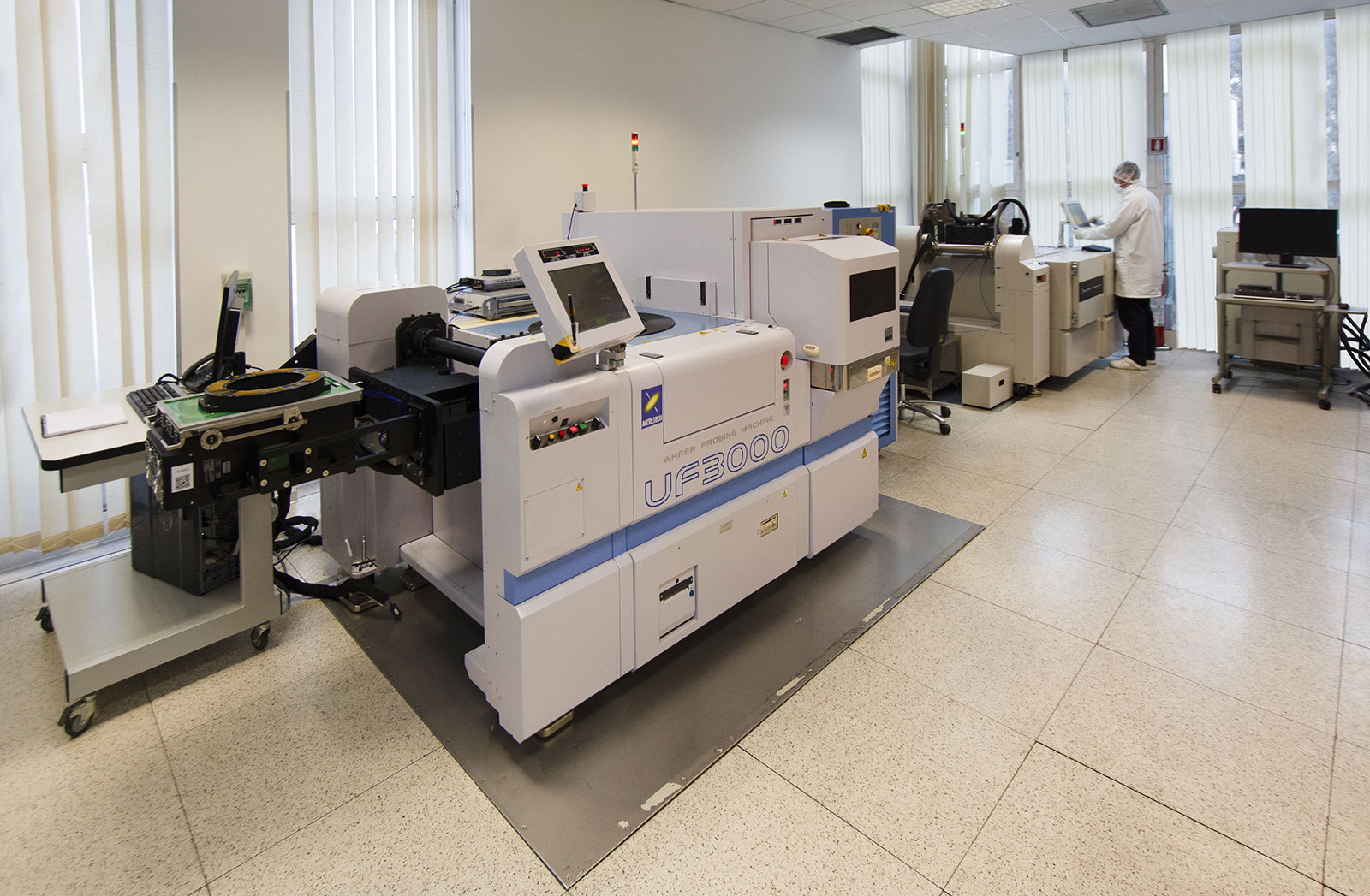
- Wafer Prober from 6 to 12 inch
- Semics Opus 3
- Accretech UF3000
- Accretech APM90
- Accretech UF200
- Thermostream
Gallery
FAQ
Semiconductor Test Services encompass the entire lifecycle of testing validation activities performed on an Integrated Circuit (IC) or Application Specific Integrated Circuit (ASIC). These services are critical because they ensure the device meets all electrical, functional, and reliability specifications before mass production and use in end applications (especially in safety-critical sectors like Automotive or Aerospace). They include everything from early Design for Testability (DFT) to final Production Test and Failure Analysis (Failure Analysis).
We become an all-in-one partner solution starting from the ASIC Design phase by applying Design for Testability (DFT) principles. This proactive involvement ensures that the circuit is inherently testable, which is vital for:
- Maximizing fault coverage (the percentage of possible defects that can be detected).
- Reducing the complexity and cost of the subsequent test program development.
- Optimizing the overall time to market.
- Characterization Test (on wafer and on packaged devices): This phase performs in-depth electrical functional measurements to determine if the device has been designed correctly and how its performance varies across different conditions (e.g., PVT – Process, Voltage, Temperature). It is diagnostic and essential for design validation.
- Production Test (Wafer Sort – WS / Final Test – FT): This is the high-volume, pass/fail screening performed to ensure every device delivered meets specifications. The focus here is on efficiency, Test Time Reduction, and maximizing Production Yield.
Yes. We specialize in the in-house development and manufacturing of complete custom test solutions, including the Test Program (Software) and the necessary hardware, such as Probe Cards and Load Boards (or socket boards). This tailored approach ensures maximum accuracy and efficiency for your specific device under test (DUT).