ASIC
DESIGN
What it means to design custom integrated circuits
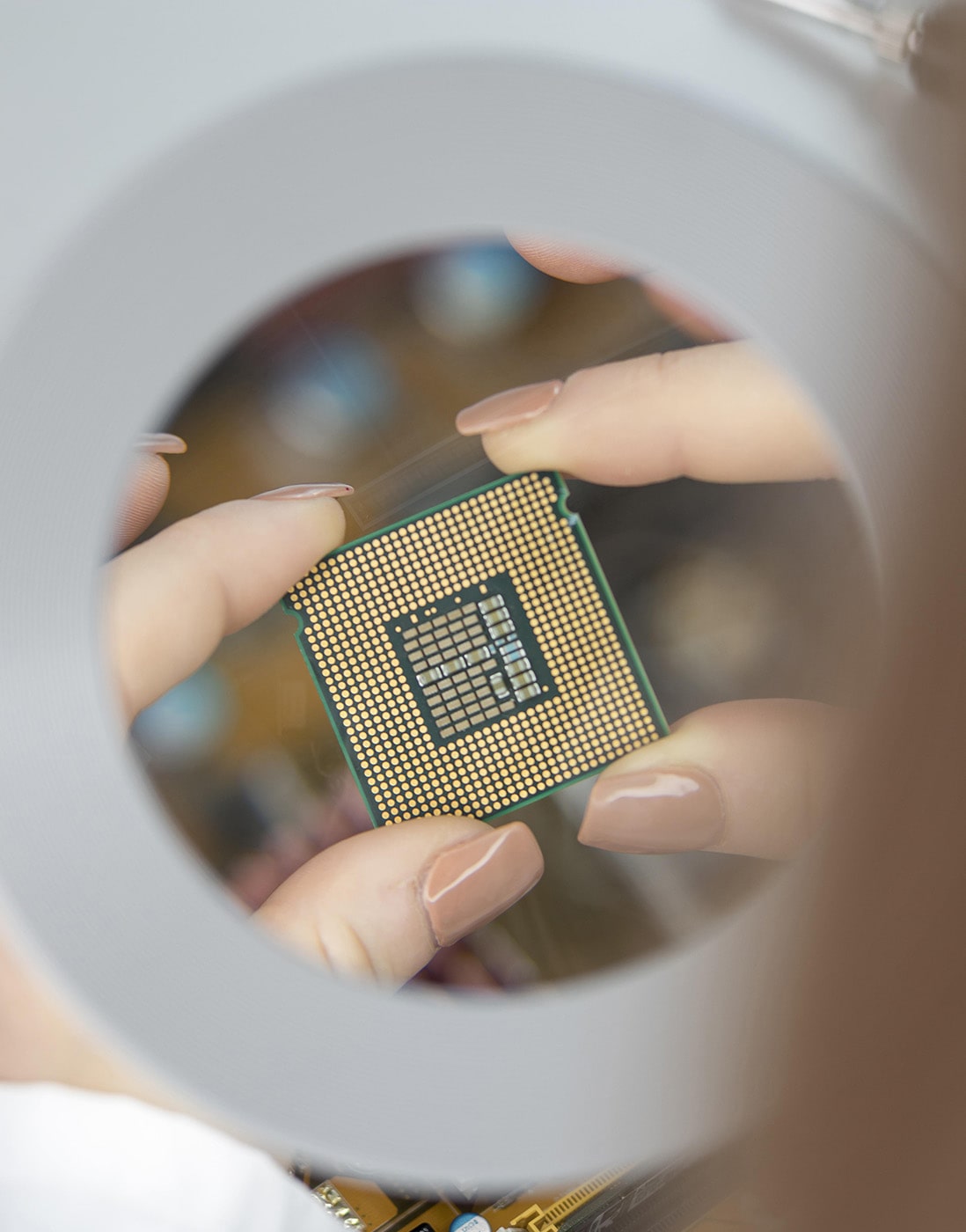
The design of ASIC (Application-Specific Integrated Circuit) represents a strategic choice for companies seeking high-performance, reliable, and customized solutions. Microtest positions itself as a technological partner for the development of custom integrated circuits, offering a comprehensive and flexible approach—from concept to final validation. Thanks to our specialized expertise and extensive industry experience, we ensure high-quality results, optimized for the specific needs of each application.
ASIC design involves the development of integrated circuits engineered to perform a specific function within an electronic system. Compared to generic components (COTS) and designs based on proprietary components (COT), an ASIC offers higher performance, lower power consumption, and a compact form factor.
ASICs leverage VLSI (Very Large Scale Integration) technologies to achieve high transistor density and ensure full integration of analog and digital circuits. This results in reliable, efficient devices optimized for critical parameters.
Features
ASIC design is a strategic discipline in the microelectronics industry: it enables the development of integrated circuits tailored to specific requirements for performance, reliability, and miniaturization, ensuring high efficiency and cost optimization throughout the entire product lifecycle.
Analog vs Digital Design: Two Worlds to Integrate
In custom integrated circuit design, the synergy between analog design and digital design is key to achieving high-performance ASICs capable of meeting demanding requirements for precision, speed, and reliability.
Analog design handles continuous signals in both time and amplitude, typically derived from the conversion of real-world physical quantities—such as temperature, pressure, and light—into usable electrical signals, or intended to drive specific transducers. Designing analog circuits requires careful consideration of numerous factors that can affect final performance, including process variability, operating temperature, piezoelectric effects, coupling, and parasitic components introduced by the fabrication technology. This activity operates at the level of individual elementary components—transistors, resistors, capacitors—which must be precisely sized to ensure proper circuit operation.
Digital design focuses on the management of discrete signals in both time and amplitude. This characteristic enables high noise immunity and significantly increases signal processing capabilities within a given area, allowing for the implementation of even highly complex functions in extremely compact spaces. The design is carried out at a descriptive level, defining functionality and behavior through languages such as VHDL. Key challenges include meeting timing constraints, particularly under worst-case process conditions. Since digital design relies on discrete signals, interface analog circuits—such as ADCs (Analog-to-Digital Converters)—are necessary to convert continuous real-world signals into quantized digital signals. Similarly, to drive transducers or actuators, DACs (Digital-to-Analog Converters) are essential to transform digital output signals into analog ones.
The fusion of these two domains enables the creation of mixed-signal ASICs: integrated solutions capable of combining analog sensitivity and precision with digital programmability and flexibility. This integration is now essential in sectors such as medical, automotive, and industrial.
What’s Inside an ASIC: Design and Layout of Integrated Circuits
The Technologies: How an ASIC Is Made
At the core of CMOS technology is the MOSFET (Metal-Oxide-Semiconductor Field-Effect Transistor), a field-effect device with a gate insulated by a thin oxide layer. MOSFETs come in two complementary types: NMOS (N-channel) and PMOS (P-channel), used together to form CMOS logic, optimizing both power consumption and performance.
In the consumer electronics market, the dominant technology for ASIC manufacturing is CMOS (Complementary Metal-Oxide Semiconductor), which is based on the use of MOSFET transistors. The strength of CMOS lies in its ability to integrate an increasing number of transistors per unit area, enabled by a process known as scaling. This has led to the development of VLSI (Very Large Scale Integration, up to 10⁹ transistors per chip) and ULSI (Ultra Large Scale Integration, up to 10¹⁰ transistors per chip). However, physical limits of scaling are emerging due to short-channel effects, which increase static power dissipation. To continue miniaturization, new technological solutions are being explored, such as high-k dielectric materials, high-mobility substrates, and innovative architectures like SOI (Silicon On Insulator) technology and multi-gate devices.

A CMOS ASIC is fabricated starting from a substrate, typically of P-type (in n-well CMOS technology). Initially, N-doped areas (n-wells) are formed to host the P-MOS transistors. A field oxide layer is then grown to electrically isolate the inactive areas. On the active areas, a thinner oxide layer (gate oxide) is created, over which polysilicon is deposited to form the transistor gate. The regions not covered by this layer are doped to create the active zones: N+ for NMOS transistors (directly on the substrate) and P for PMOS (within the n-well).
Next, a vapor-phase-deposited insulator is applied and selectively removed in contact areas, followed by metallization, which connects the gate and active regions. Additional layers of oxide and metal can be added to create multiple interconnections, ending with a passivation layer that is removed only over the contact pads, which connect the chip to the package pins via bonding wires.
From Concept to Chip: The Phases of IC Design
ASIC design is a process composed of multiple phases, each of which is crucial to the success of the ASIC itself:
The ASIC design process begins with a detailed analysis of the specification, based on the device’s datasheet and application requirements. The datasheet serves as the reference document defining the electrical parameters and functionalities, forming the foundation for all subsequent design decisions.
Based on the specification, the designer defines the overall architecture of the ASIC by dividing it into functional blocks. Each block represents a circuit implementing a specific function. The design follows a hierarchical approach, with different “views” associated with each block:
- Schematic view: represents the circuit through the interconnection of elementary components such as MOSFETs, resistors, and capacitors.
- Symbolic view: shows only the terminals of the block, simplifying interconnection with other blocks.
This modular approach simplifies system complexity management and ensures a more structured and scalable design.
Schematic design begins with the definition of the block’s functionalities and interface signals. Using a design editor integrated with the foundry-provided design kit, the designer selects components available in the chosen technology.
The circuit is then simulated to verify its behavior and performance against the specification. Simulations use accurate component models included in the design kit and enable optimization of component sizing.
Simulations also include checks for:
- Design for Testability (DfT): the inclusion of auxiliary structures to improve testability, such as analog test-mode multiplexers and controlled switches for signal measurement during testing.
- Design for Reliability: techniques adopted to ensure long-term reliability, such as aging simulations to evaluate parameter drift and the implementation of circuits to mitigate such effects.
- Design for Robustness: design practices to ensure robustness against phenomena such as ESD (Electrostatic Discharge) and EMC (Electromagnetic Compatibility).
To ensure the quality and reliability of the ASIC, specific test strategies are implemented:
- Internal testability: critical voltages and currents are routed to the top level of the ASIC through analog multiplexers, allowing measurements during testing without affecting functional performance.
- Stress testing: application of stress voltages to critical components, such as power MOSFETs, to detect latent defects. During these tests, connected circuitry is isolated using controlled switches.
- Leakage testing (IDDQ test): measurement of leakage currents to identify defects in CMOS devices. To ensure test effectiveness, currents from analog blocks are disabled and floating nodes are forced to known potentials.
These strategies are essential to ensure that the ASIC performs reliably over time and under real operating conditions.
ASIC Design Phases: From Concept to Production
The layout physically defines the chip, translating the design into process masks that guide fabrication. The floorplan determines the optimal arrangement of macro blocks, ensuring physical and electrical separation between noisy blocks (e.g., oscillators, switching regulators) and sensitive ones (e.g., voltage references, monitors). This includes duplicating power supply traces, using dedicated ground planes, and minimizing trace lengths to reduce parasitic resistance and enhance reliability.
Advanced tools perform checks for compliance with technology rules (Design Rule Checker – DRC) and verify correspondence between layout and schematic (Layout Versus Schematic – LVS).
The layout introduces parasitic resistances and capacitances that affect final performance. Dedicated software tools extract these parameters, creating an “extracted view” of the circuit, which includes parasitic coupling between traces and to ground. Post-layout simulations use this view to assess the impact of parasitics and guide necessary adjustments: widening overly resistive traces, relocating noisy nets, and applying corrections to improve signal integrity.
Digital ASIC design is divided into two main phases:
- Front End:
- Functional and logic design at the RTL level (using languages such as VHDL or Verilog).
- Insertion of testability structures (Design for Test, scan chains, BIST).
- Functional and test simulations to validate logic before synthesis.
- Back End:
- Logic synthesis: conversion of RTL logic into a gate-level netlist, including insertion of Digital BIST and scan chains.
- Verification: test coverage and formal verification to ensure RTL-to-synthesis consistency.
- Physical layout: placement, clock tree synthesis, routing, parasitic extraction.
- Final checks: timing analysis, power analysis, DRC and LVS to ensure compliance with design rules.
- Post-layout: final simulations, verification of test coverage, and generation of test patterns for ATE.
Simulations integrating both analog and digital blocks, performed on the entire ASIC powered and stimulated through external pins. They verify system consistency, correct communication between blocks, and operational stability under real-world conditions, including fault scenarios.
Production begins with the .gds file containing all layout information. Silicon wafers are processed to form the circuits, then diced to obtain individual dies. Each die is mounted on a metal frame and connected via bonding wires to the package pins, which is then sealed with plastic or ceramic resins to form the complete ASIC.
The completed ASIC moves to the validation phase, during which the designer performs functional tests on dedicated evaluation boards to verify compliance with specifications. In parallel, the test engineer carries out characterization using ATE, measuring electrical parameters and calculating the Cpk index, which provides insight into production capability and the stability of the industrial process.
If validation or characterization reveals discrepancies from the specifications or a Cpk value that is too low, a re-design is carried out. This phase allows for circuit optimization and ensures full compliance with the requirements, guaranteeing robustness and production yield.
The final qualification of the ASIC involves rigorous testing, such as those defined by the AEC-Q100 standard for the automotive sector. The device is subjected to cycles of temperature, pressure, and humidity to verify the stability of critical parameters. These tests simulate extreme operating conditions and confirm the robustness and stability of the ASIC and its package, certifying its suitability for the intended application.
Custom ASIC Design Success Stories
Discover how tailored integrated circuits have transformed performance, efficiency, and reliability across industries, from concept to silicon, with Microtest’s end-to-end ASIC expertise.


Get in touch
Glossary
-
ASIC (Application-Specific Integrated Circuit)
An integrated circuit designed and manufactured to perform a specific, optimized function within an electronic application. Unlike standard circuits, it offers high performance, energy efficiency, and full customization.
-
MOSFET (Metal-Oxide-Semiconductor Field-Effect Transistor)
A field-effect transistor with a gate insulated by a thin oxide layer. It is the fundamental component of CMOS technology, known for its fast switching capability and low static power consumption.
-
CMOS (Complementary Metal-Oxide Semiconductor)
A technology that combines NMOS and PMOS transistors to reduce static power consumption and increase the efficiency of integrated digital and analog logic circuits.
-
VLSI (Very Large Scale Integration)
An integration technology that enables the implementation of circuits with hundreds of millions of transistors on a single chip, ensuring compactness and high performance.
-
ULSI (Ultra Large Scale Integration)
An evolution of VLSI that enables surpassing the threshold of one billion transistors per chip, pushing miniaturization and circuit complexity to extreme levels.
-
Layout
A detailed physical representation of the integrated circuit, including process masks, metallization layers, contact areas, and isolations. It is the final step before foundry production.
-
Floorplan
The phase of placing functional blocks within the ASIC, focusing on physical and electrical separation between sensitive and noisy areas, minimizing trace lengths, and optimizing power distribution.
-
ESD (Electrostatic Discharge)
An electrostatic discharge phenomenon that can damage electronic components. ESD protection is essential for ensuring the device’s robustness and long-term reliability.
-
EMC (Electromagnetic Compatibility)
The ability of a circuit to operate without causing or being affected by interference from other electronic systems. It involves both minimizing electromagnetic emissions and withstanding external disturbances.
-
Drift / Aging
Gradual variation of a device’s electrical parameters over its lifetime, caused by material aging and operational stress phenomena.
-
Design for Testability (DfT)
A design approach that involves the insertion of dedicated circuitry and interfaces to facilitate testing, improve test coverage, and reduce verification costs.
-
ATE (Automatic Test Equipment)
Advanced automated equipment for testing electronic devices, used during characterization and production phases to measure performance and verify compliance with specifications.
-
Cpk (Process Capability Index)
A statistical index that measures the production process capability to keep device parameters within specification limits, representing a direct indicator of industrial quality.
-
FIT (Failure In Time)
A parameter expressing the failure probability of a component per billion hours of operation, used to quantify long-term reliability.
-
SIL (Automotive Safety Integrity Level)
A classification indicating the safety level required for an electronic device in automotive applications, with four increasing levels (A–D) based on criticality and safety requirements.
-
DFMEA (Design Failure Mode and Effects Analysis)
A qualitative analysis of systematic faults and their effects on ASIC operation, based on parameters such as severity, detection, and occurrence.
-
DFMEDA (Design Failure Mode, Effects and Diagnostic Analysis)
A quantitative analysis of random faults and the diagnostic coverage of integrated monitors and protection mechanisms.

