Hatina WLBI

Solution for wafer level Burn-In for power MOS
Reasons Why


Product Presentation
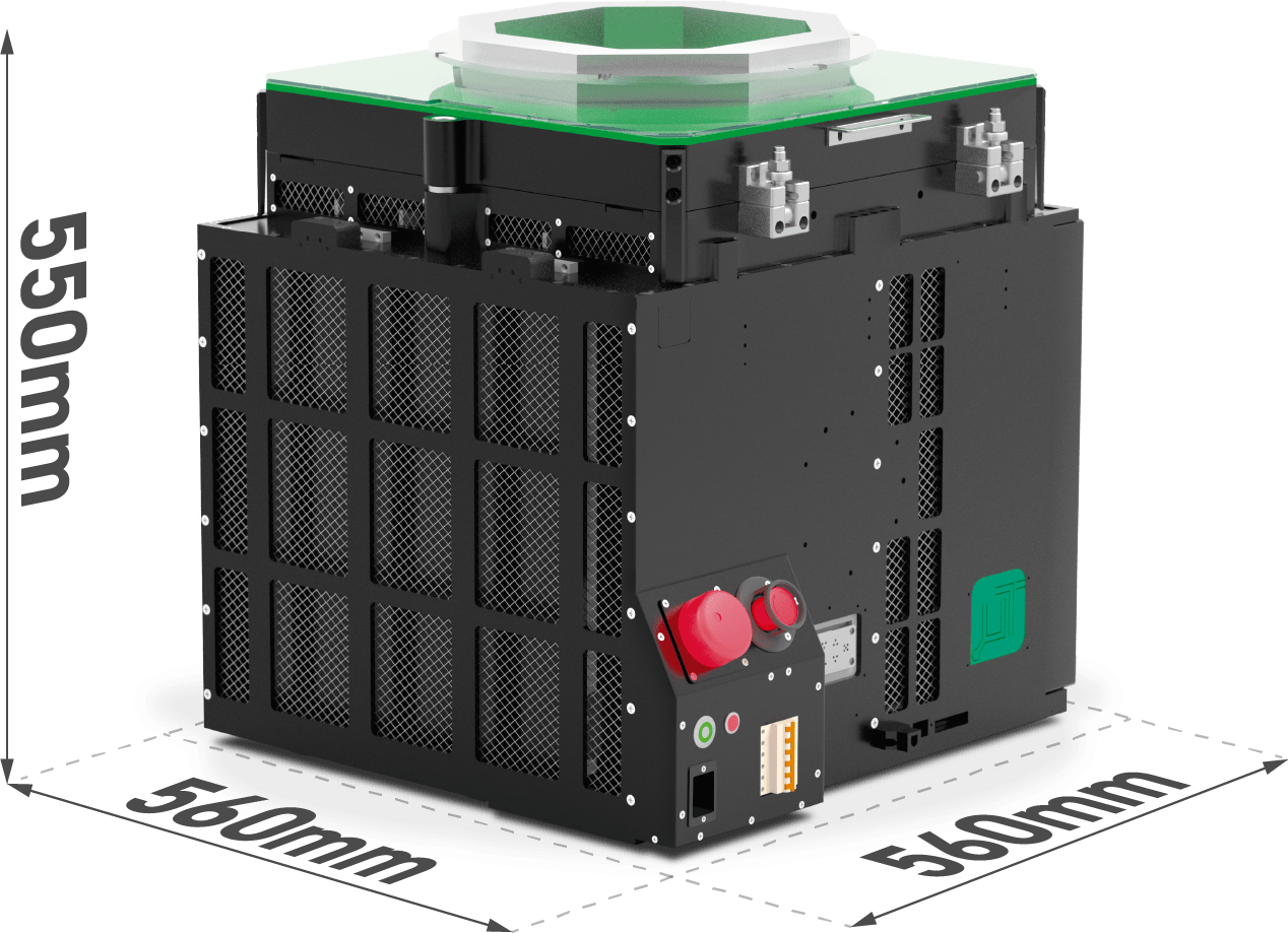
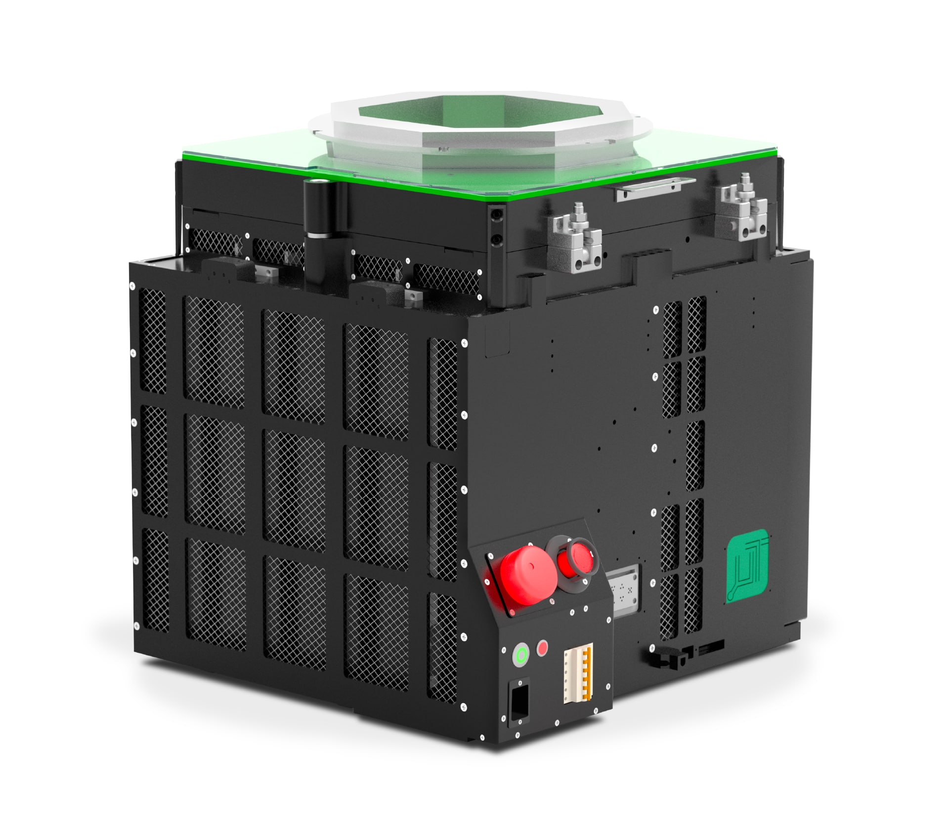
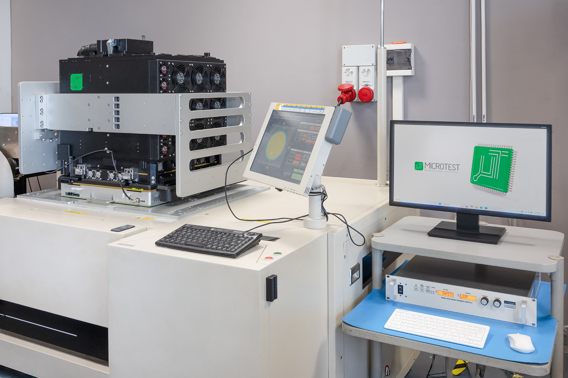
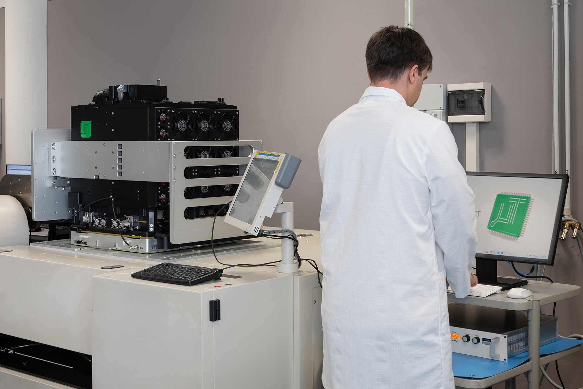
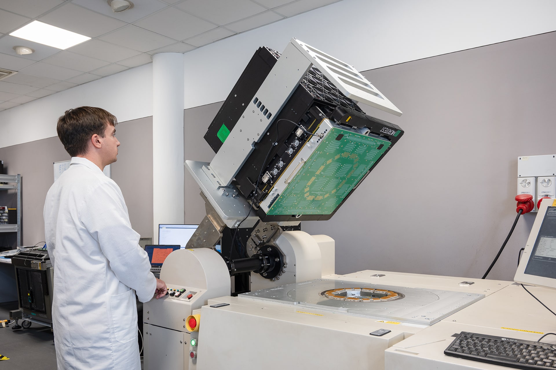
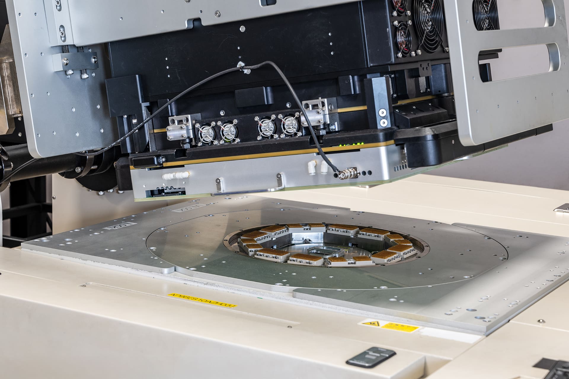
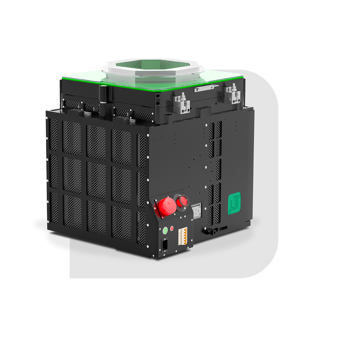
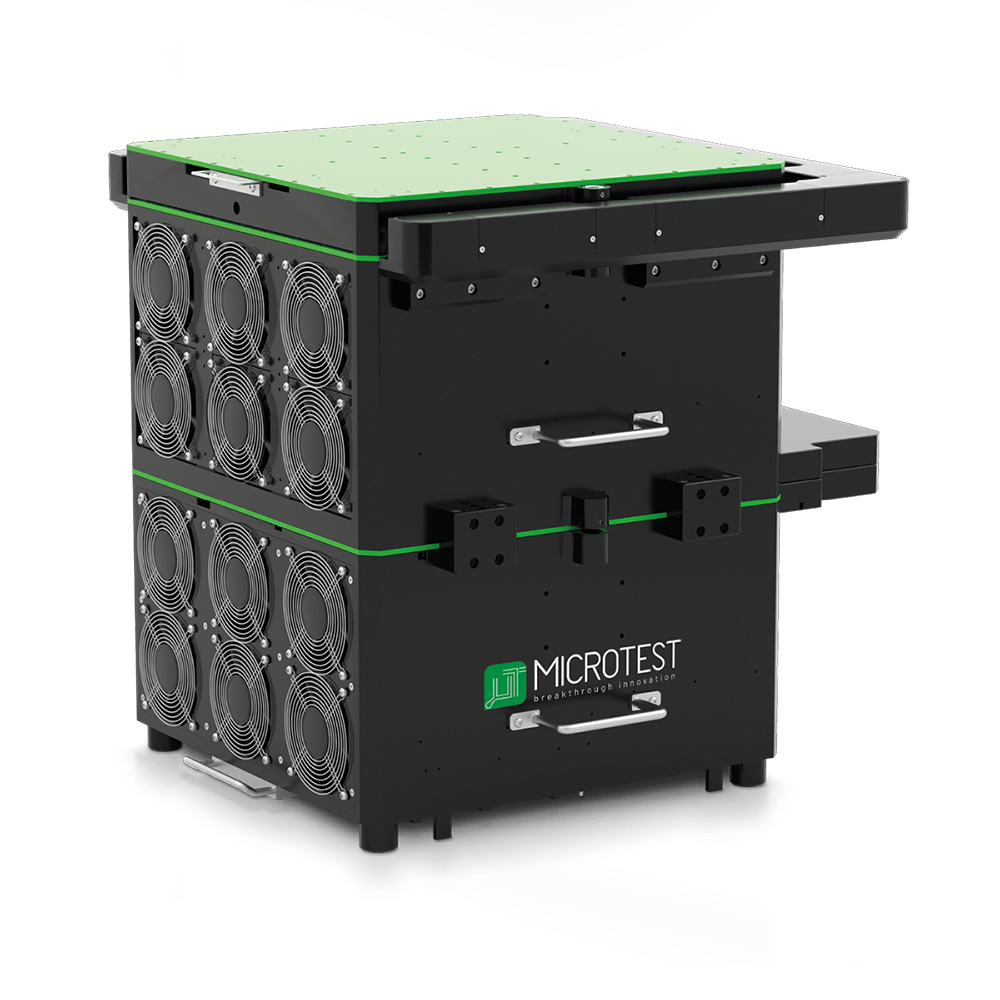
The Hatina WLBI by Microtest is a robust wafer-level Burn-In and HTOL (High-Temperature Operating Life) solution designed specifically for power devices on wafers. This compact test chamber (560×560×550 mm) plugs into standard wafer probers, enabling full-wafer Burn-In without major equipment overhauls.
Its high parallel throughput supports up to 1,600 test sites simultaneously, each operating at up to 1.2 kV and 2 mA—ideal for lifecycle and reliability testing of power technologies.
The WLBI seamlessly integrates functional burn-in, HTGB (High-Temperature Gate Bias), and HTRB (High-Temperature Reverse Bias) test setups, offering a flexible and cost-effective package.
Compact and easy to handle, the WLBI is engineered for cleanroom use and aligns with Microtest’s ovenless Burn-In philosophy—embedding heaters directly at each DUT for precise, low‑power thermal control.
This design reduces energy use, lowers footprint, and simplifies automation compatibility.
In summary, the Hatina WLBI is a high-density, wafer-level Burn-In platform that delivers full-wafer reliability testing for advanced power semiconductors, combining high voltage, tight temperature control, and multi-site scalability in a compact, integration-friendly format—perfect for enhancing manufacturing efficiency and device confidence.
Hatina WLBI
Dimensions
Analog/Power
Applications

Gallery
More info
Related Products

This App allows you to visualize some 3D models of Microtest ATE in Augmented Reality.
