Hatina WLBI

Soluzione per il Burn-In a livello wafer di MOS di potenza
Reasons Why


Product Presentation
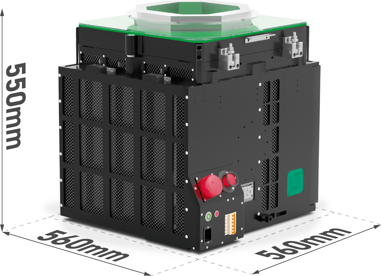
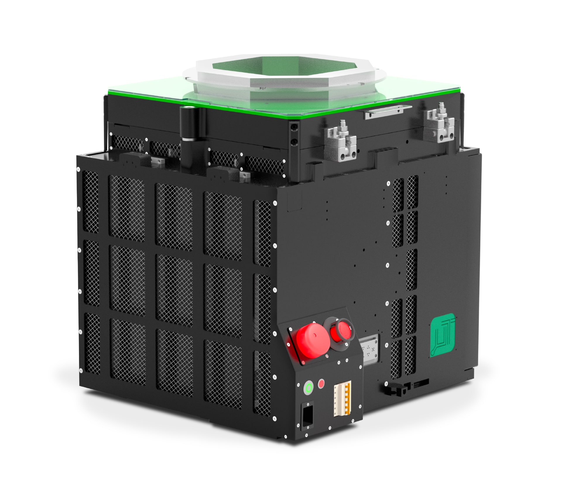
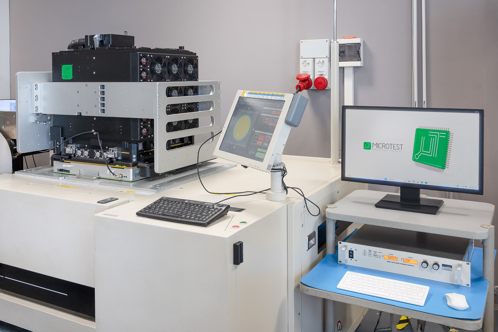
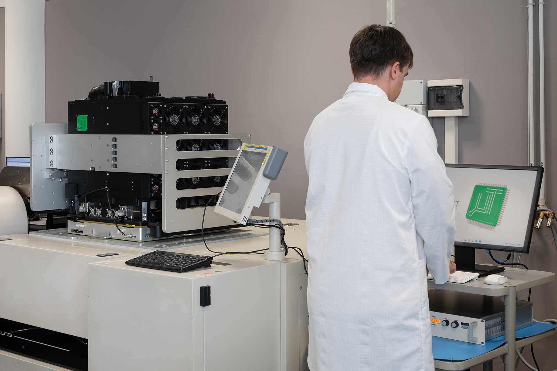
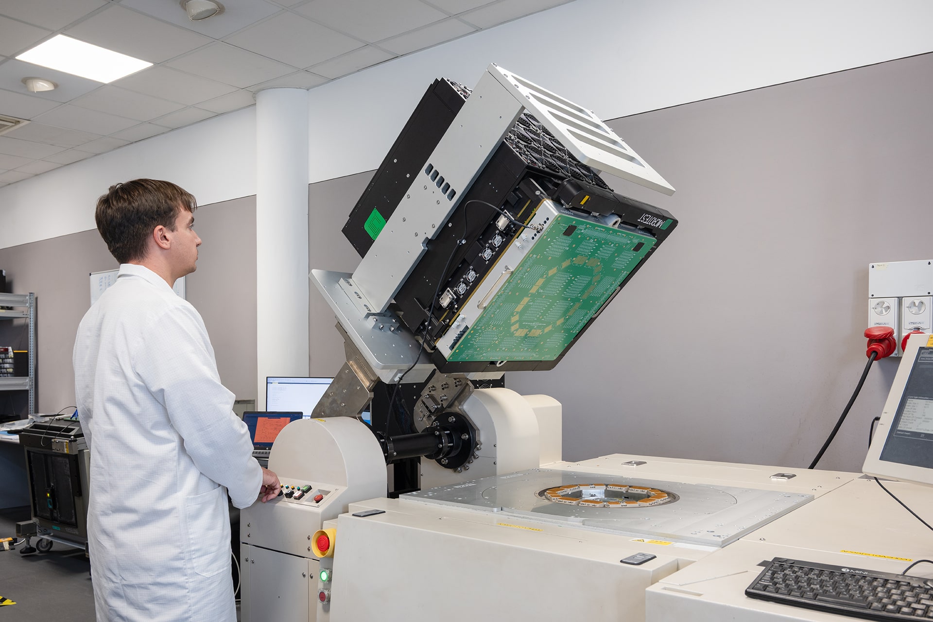
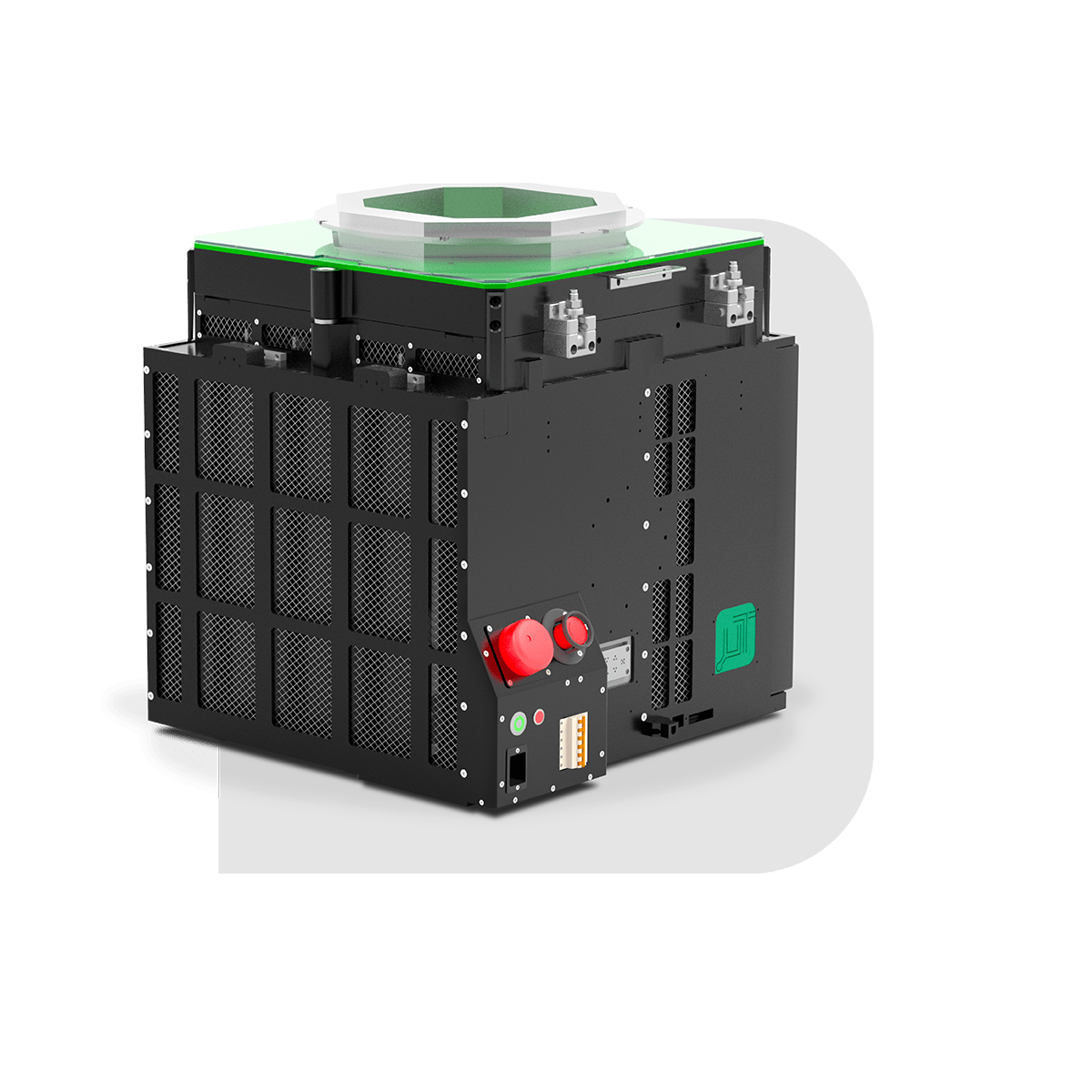
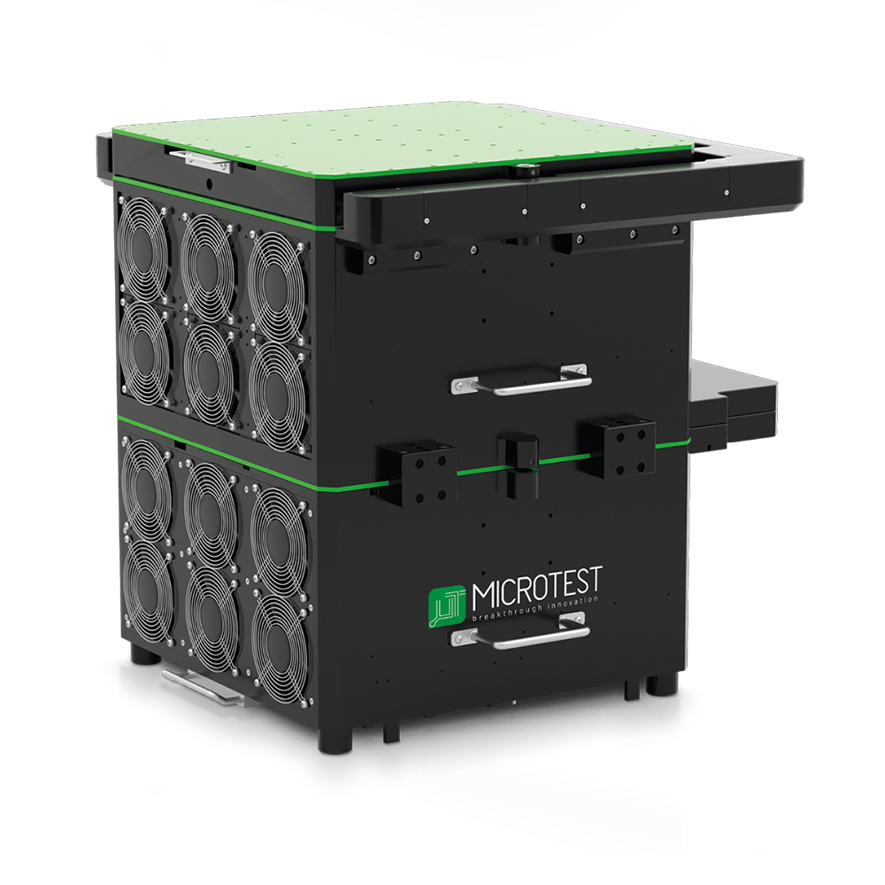
Hatina WLBI di Microtest è una soluzione robusta per Burn-In e HTOL (High-Temperature Operating Life) a livello wafer, progettata specificamente per dispositivi di potenza su wafer. Questa camera di test compatta (560 × 560 × 550 mm) si collega direttamente a prober standard per wafer, consentendo il Burn-In su wafer intero senza necessità di modifiche significative alle apparecchiature esistenti.
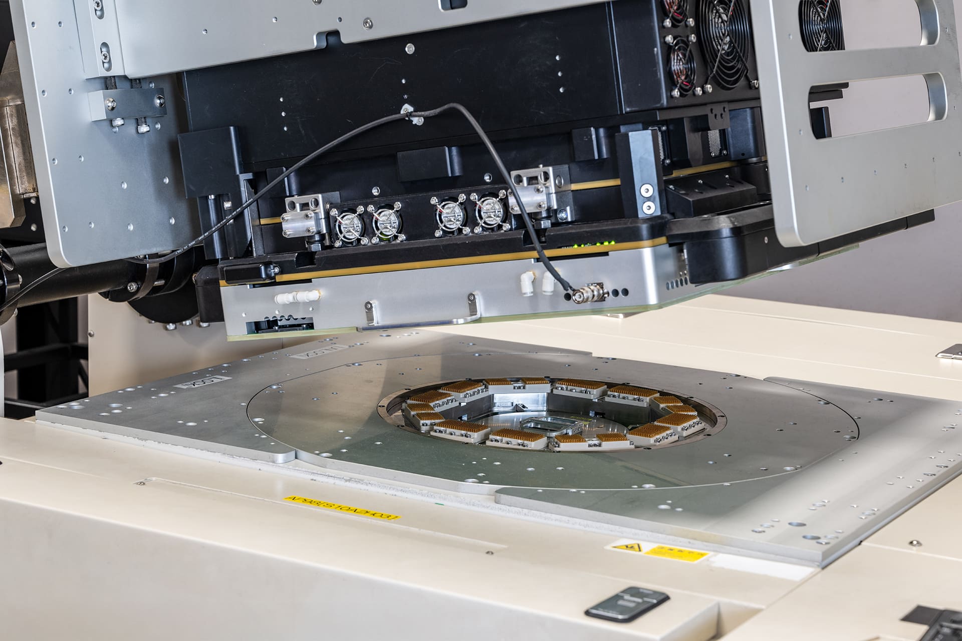
Il sistema supporta un’elevata produttività in parallelo, con la possibilità di gestire fino a 1.600 siti di test simultaneamente, ciascuno operante fino a 1,2 kV e 2 mA, ideale per test di affidabilità e durata nel tempo delle tecnologie di potenza.
WLBI integra perfettamente setup di test per Burn-In funzionale, HTGB (High-Temperature Gate Bias) e HTRB (High-Temperature Reverse Bias), offrendo un pacchetto flessibile ed economico.
Compatto e facile da gestire, WLBI è progettato per l’uso in camera bianca e rispecchia la filosofia di Microtest del Burn-In senza forno, grazie a riscaldatori integrati direttamente su ciascun DUT per un controllo termico preciso e a basso consumo.
Questa architettura consente di ridurre i consumi energetici, minimizzare l’ingombro e semplificare l’integrazione nei sistemi di automazione.
Hatina WLBI è una piattaforma Burn-In ad alta densità a livello wafer, che consente test di affidabilità completi su wafer interi per semiconduttori di potenza avanzati. Combina alta tensione, controllo termico preciso e scalabilità multisito in un formato compatto e facilmente integrabile, perfetto per aumentare l’efficienza produttiva e la sicurezza dei dispositivi.
Hatina WLBI
Dimensions
Analog/Power
Applicazioni

Gallery
Maggiori Informazioni
Prodotti Correlati

Questa app permette di visualizzare alcuni modelli 3D degli ATE Microtest in Realtà Aumentata.
